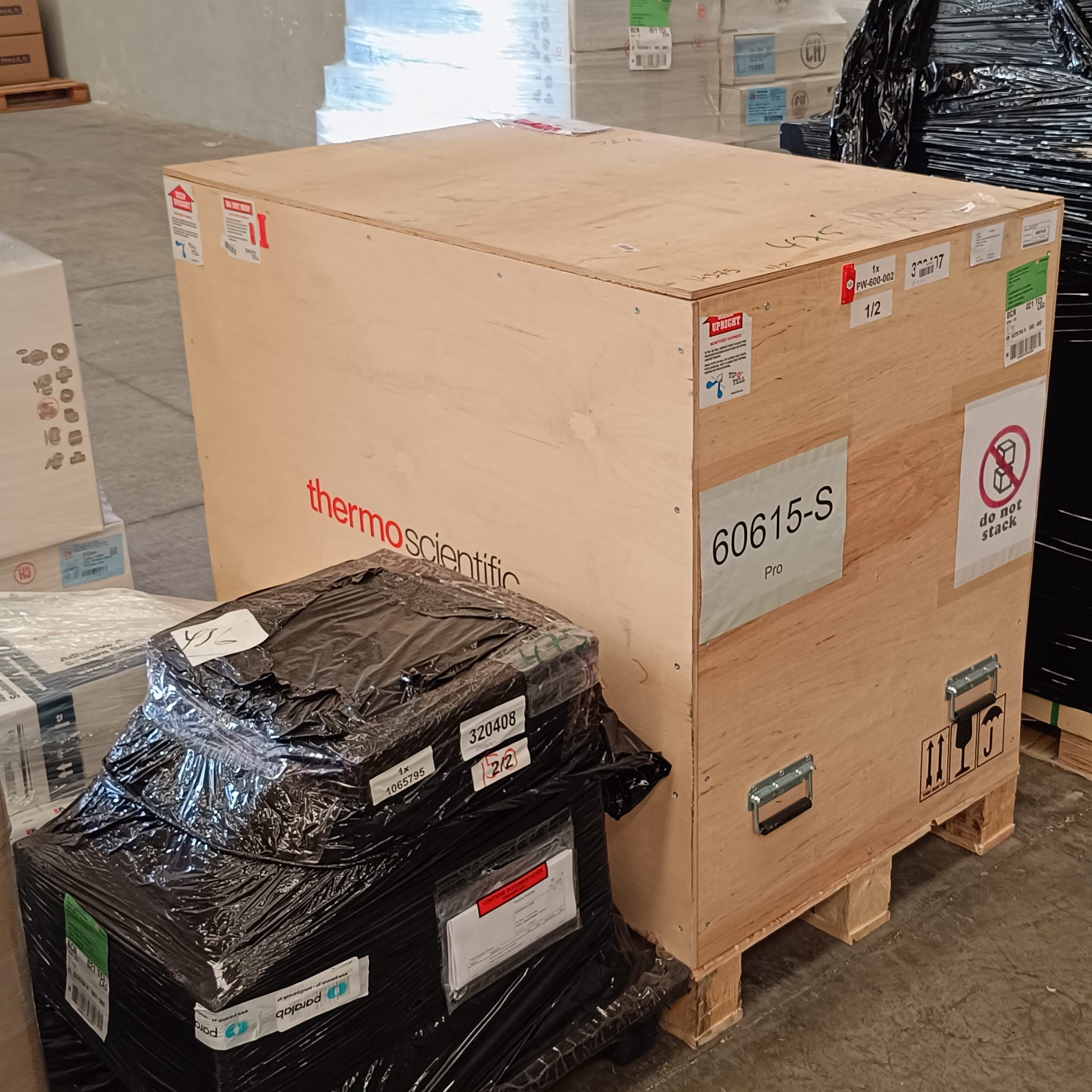
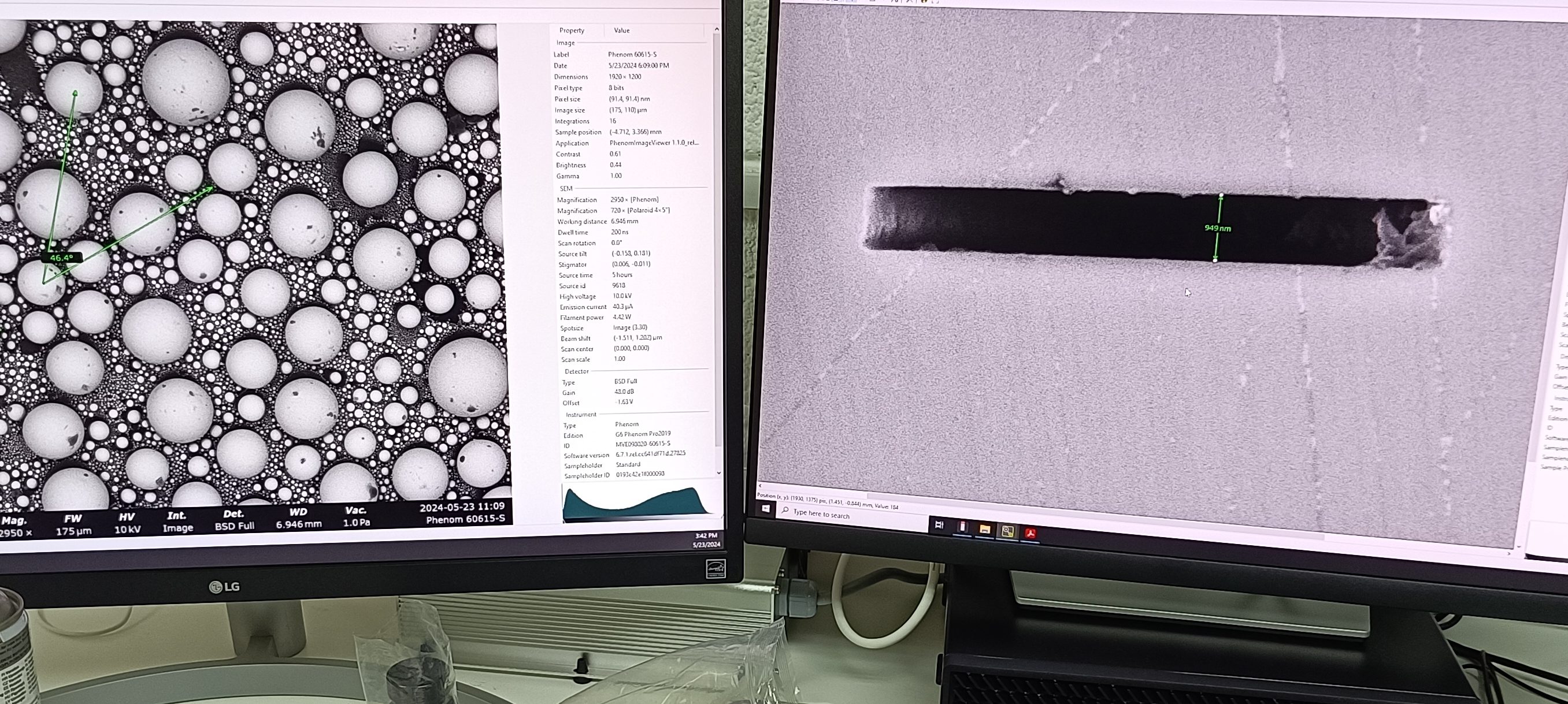
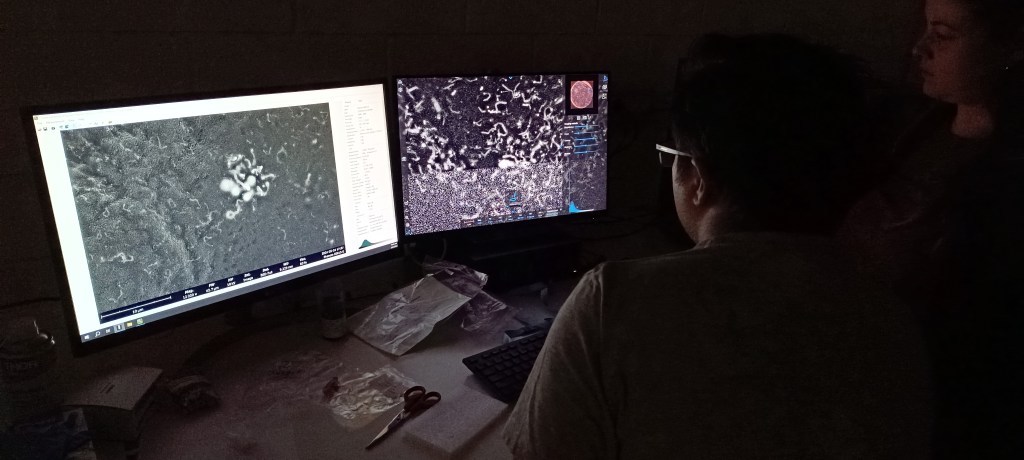
24th May 2024. A new Scanning Electron Microscopy (SEM) system has been installed at LeapLab’s laboratories this week of May 2024.
“This new equipment will now allow us to directly characterize materials in situ in our labs without the need to change buildings, book in external services and wait for weeks etc. Our own nanofabrication protocols and workflows are now complete from design to characterization. We can now perform laser nanolithography, postprocessing, and sample characterization all on the fly. It has taken a full year of paper work to acquire the system but we are now all set to boost our laboratory productivity”, said Dr. A. Ródenas, supervisor of the LeapLab.